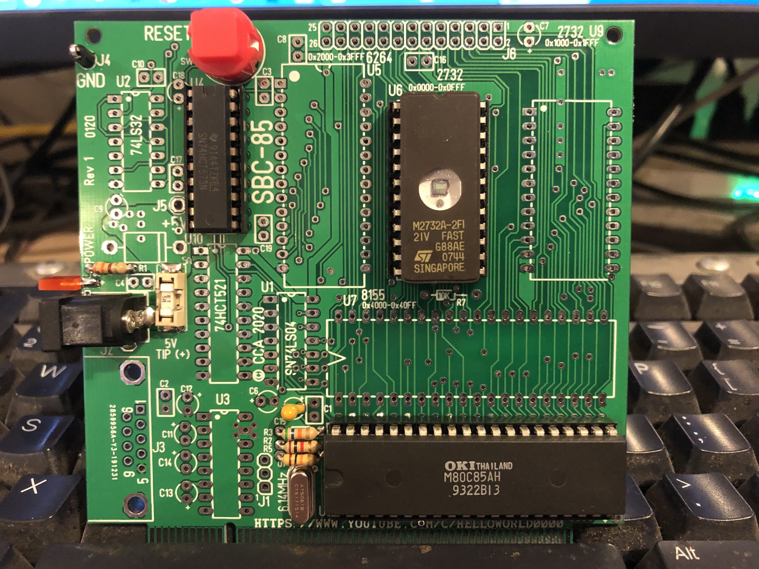
UPDATE: The SBC-85 CPU v2 is now available.
Those that do not have 21V programmers for the 2732A, or those running CP/M and other high memory requirements can rejoice. Version 2.0 (previously identified as v1.3) of the SBC-85 CPU board will soon be completed and tested.
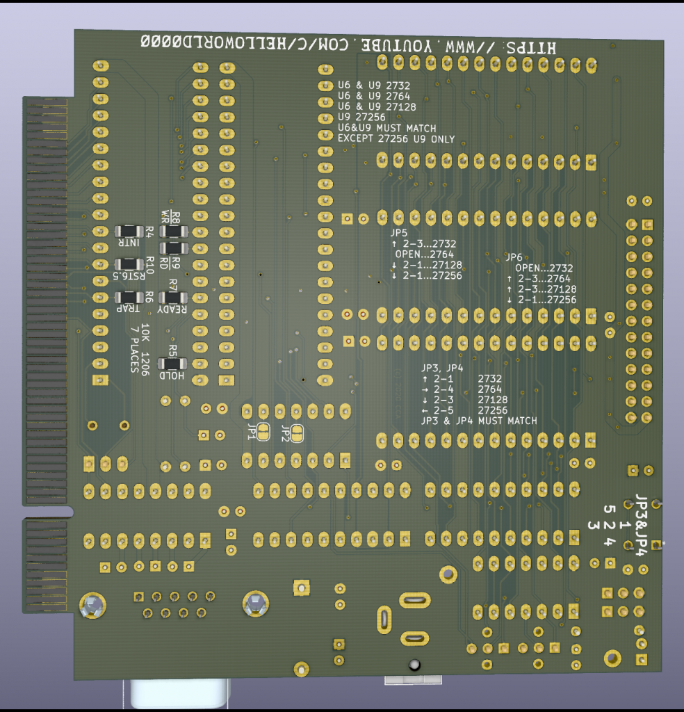
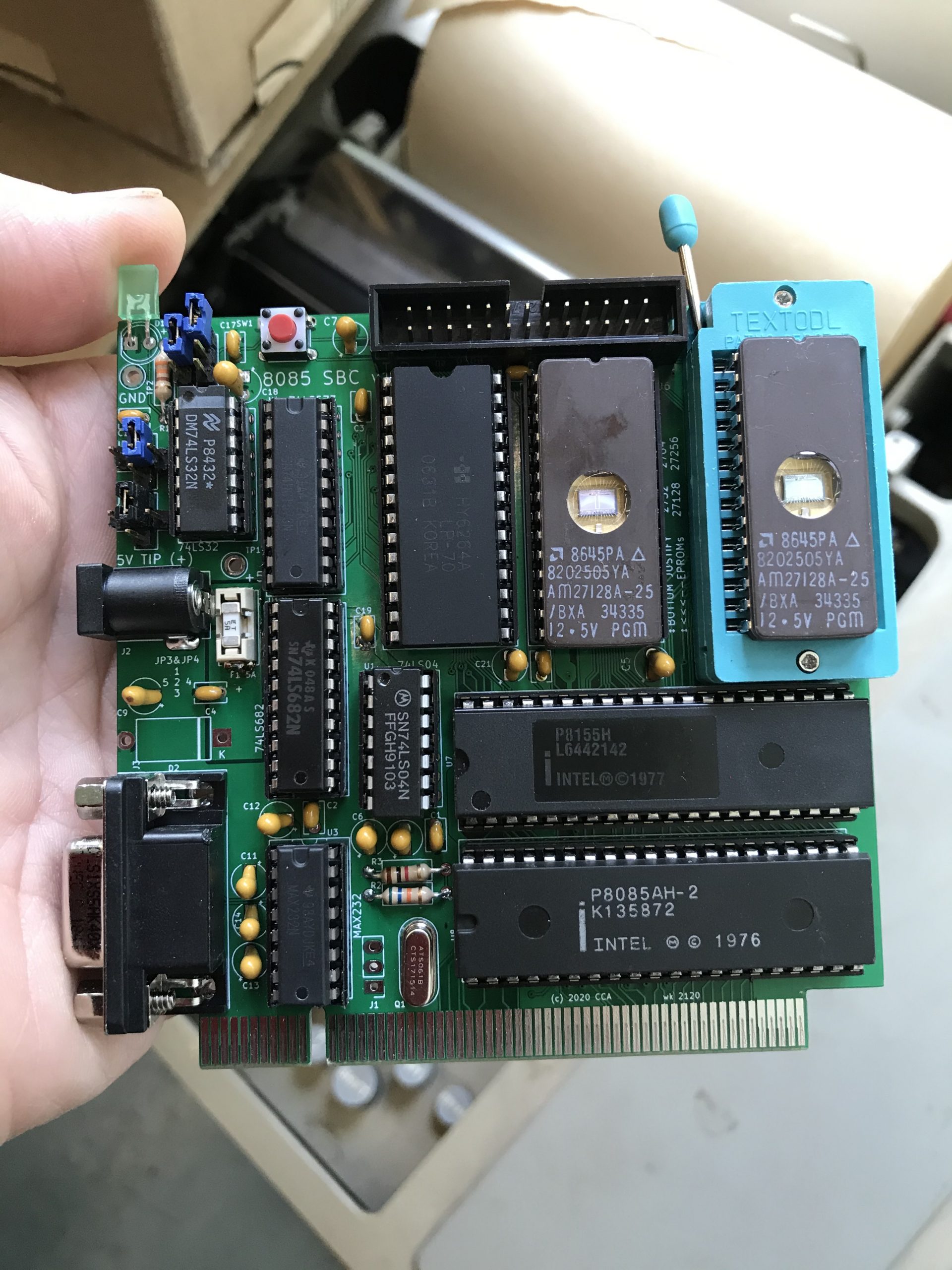
When I first did the layout on v1.0, I did not think there would be room for any EPROM larger than the 24 pin 2732 and certainly not room to put the expansion EPROM into a ZIF socket. However, I optimistically created the schematic with 28-pin universal EPROM sockets, added the requisite jumpers, and began the long process of getting it to fit in the same 100mm x 100mm footprint. Quite to my surprise, I was able to get dual 28 pin EPROM sockets and still have room for the ZIF on the expansion EPROM. The routing had to be restarted several times and in some places the trace spacing had to decrease but the minimum trace width is still 10mil. With the narrower gap, however, this means that the board will be somewhat more expensive to manufacture at any of the houses that charge extra for 5 mil spacing.
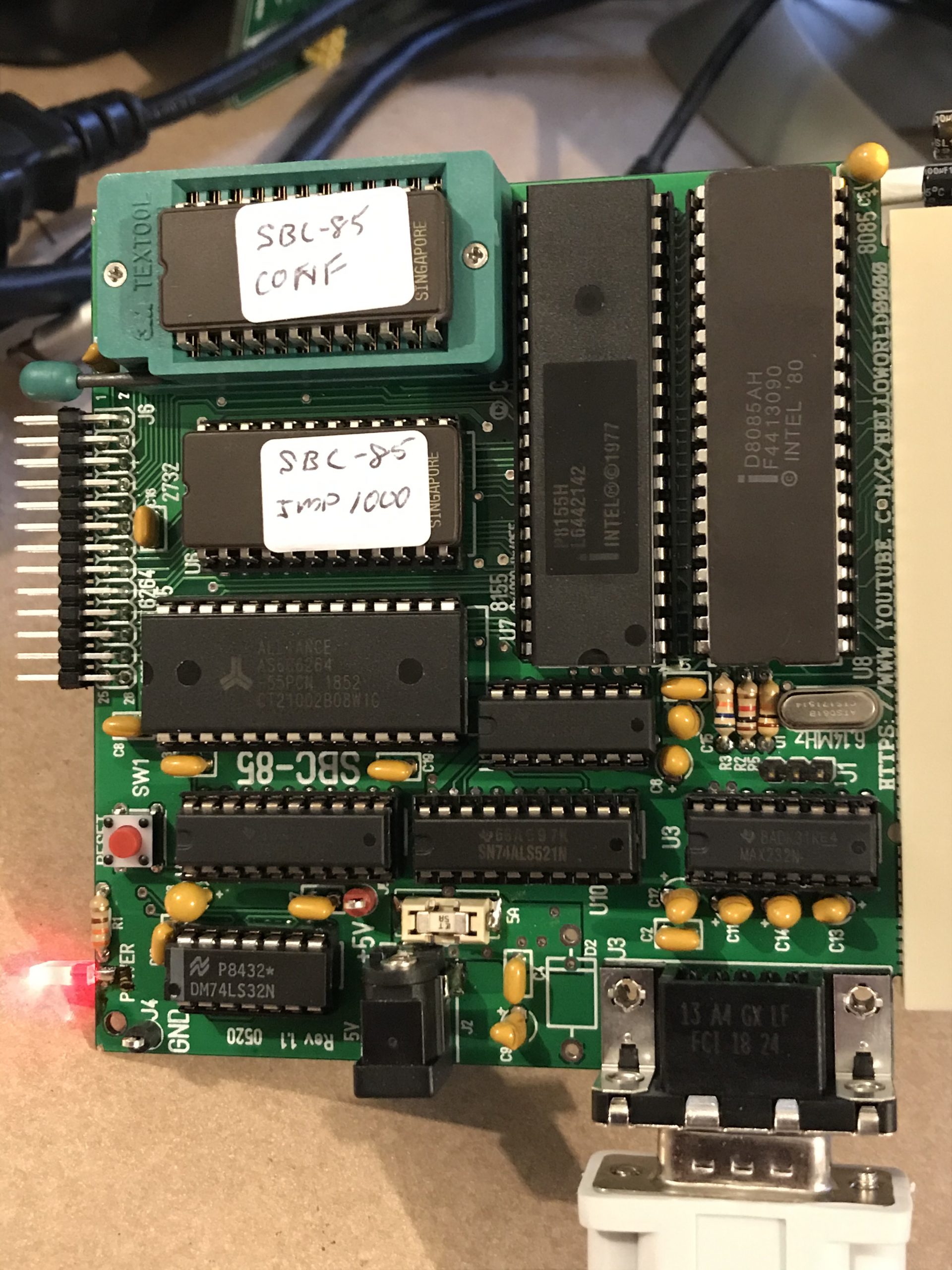
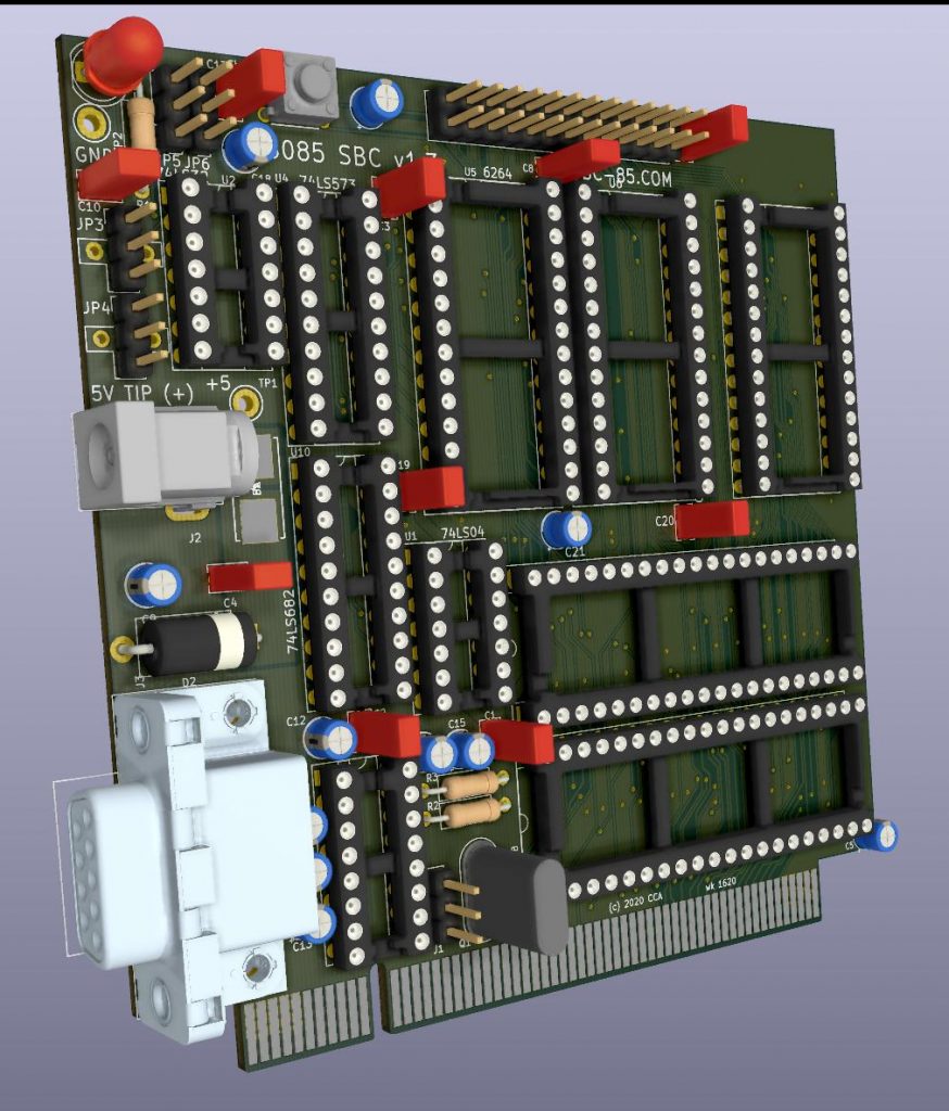
As can be seen from the image, the general placement of all components has remained the same but the 24-pin EPROM sockets are now 28-pin universal EPROM sockets and two sets of jumpers for device selection have been added in the top left portion of the board. While both EPROMs have to be the same size, this board accepts a pair of 2732s, 2764s, or 27128s or the board can accept a single 27256 in the ZIF socket. All other features of the board remain pretty much unchanged, with the 8155 and its 22-pins of I/O, the MAX232 serial port, and the full backplane expansion. Version 2.0 also brings RESET and RESET* to the backplane which was an oversight on the first versions.
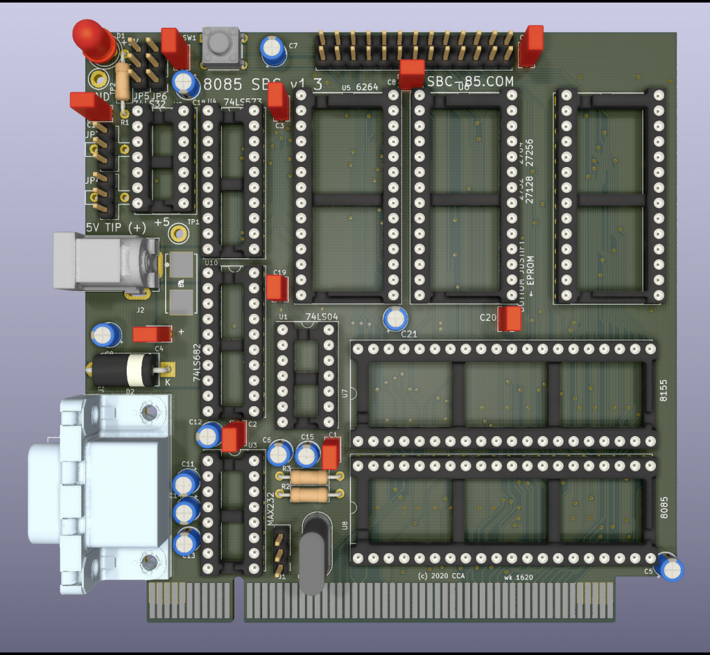
In addition to the difficulty of simply getting this all to fit on a 100mm x 100mm 2-layer board, the new memory flexibility also created address decoding headaches. It was important to keep the address decoding straightforward yet avoid holes in the memory space and to avoid stepping up to programmable logic device. In the end, I was able to make the EPROM address space contiguous for all possible configurations, move the RAM up to a higher address, and create the hole in between the EPROMs and RAM. In version 1.3 the EPROM memory space still begins at 0x0000 and extends up to their maximum combined address, but the RAM has been moved from 0x2000 up to 0x8000. If using a total of 256KBit of EPROM the top of ROM still bumps up against the bottom of the RAM. If using less than the maximum EPROM on this board, then there is a memory hole but rather than scattered memory it is a single hole that can easily be filled by the memory expansion board as RAM or ROM. To be more specific, in version 1.3 the 6264 RAM is now from 0x8000 to 0x9FFF, the 8155 is enabled from 0xA000 to 0xA7FF, and the 8155 ports begin at I/O 0xA0.
With the 32KB of EPROM available on the CPU board plus [any ROM / RAM combination up to 128KB ROM or 32KB RAM] available on a memory expansion board, the SBC-85 should satisfy even the most hard-core memory needs. Add to that a 1Mbit bubble board and you have a pretty nice system on your hands.
I am well into creating the documentation and will upload as it becomes available in draft form. With any luck, v1.3 will be tested and a few prototypes available in June with the final version and the build files released in July. Note that the user’s manual, BOMs, and remaining documentation is being updated to include the v1.3 hardware.
