

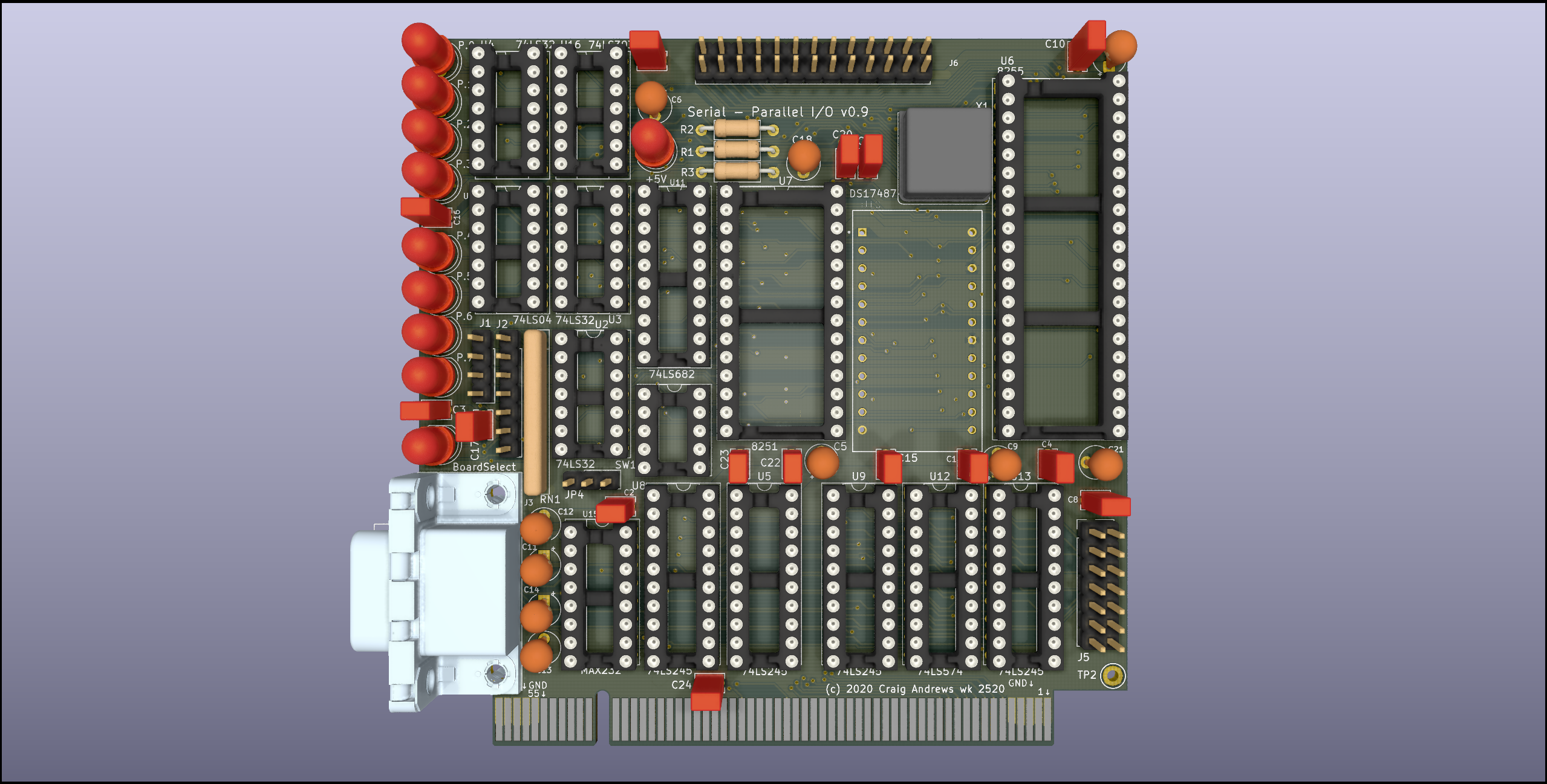
With every job at the PCB fab I like to include a prototype of a new design. This month, someone suggested a Serial & Parallel I/O card with a USART and a PPI (Programmable Parallel Interface), so the last couple of days I did the design and layout and am submitting the SPIO card to the fab house today.
The board has four I/O devices:
- An Intel 8255 PPI which provides three, 8-bit programmable I/O ports;
- An Intel 8251 USART for an RS232 serial port;
- Expansion I/O port header;
- A generic ‘from scratch’ parallel I/O port with LED bit-display.
The last one was added just because with the decoding there was a port addresses left over in the reservation that needed to be made useful rather than leaving an unused port address on the table.
The 8255 PPI has a 26 pin header that matches the 8155 I/O on the SBC-85 CPU, except the last two pins (25 & 26) are used for I/O rather than redundant power and ground. A very nice feature of the 8255 is direct bit set/reset capability and will be handy for bit-banging out to all of your I2C, Dallas 1-wire, and SPI devices. As common to all Intel parallel port devices, port C can also be used for handshaking for ports A & B if you have your eye on a Centronics style parallel port.
For those that are offended by RS232 out the 8085 SID and SOD, need another serial port, or just want more throughput than bit-banging can deliver, the 8251 USART offers an interrupt driven turn-key serial port up to 19.2K Baud. Its DB9 uses the CTS-RTS or they can (must!!) be looped with a jumper if not used. There is a little patch area where the USART buffer pins can be connected to interrupt lines, and a left over OR gate is provided if you want to hybridize the interrupt request. (Two other unused OR gates and two inverters are left with solder jumpers if you want to patch them in to something.)
Finally, the from-scratch parallel port has a 14 pin header. Buffered LED bit-wise display of the signal values is along the left side of the board for those that like blinky things.
All totaled, the board takes eight sequential port addresses with the base address set by a five position DIP. As always, I used brute force address decoding to avoid the use of any programmable devices and while decoding was straight forward it is a little bit messy since everyone needed a different number of ports. The 8255 gets the bottom four port addresses ( i.e., xxxx x0xx), the 8251 gets the next two (base + 04H & 05H, i.e., xxxx x10x), the port expansion header gets the next address (base + 06H, i.e., xxxx x110) and the roll-your-own port gets the top address (base = 07H, i.e., xxxx x111).
It was a little bit of a rush job and there are bound to be some mistakes, so if you find one please let me know. I had many other opportunities to mess up the design and layout, however, if the board does happen to work it is time to brush up on your 8251 and 8255 programming.
 v0.9 Prototype Going to Fab")


