
One tool for a healthy hardware user group is the ability for the users to create, invent, and contribute. I pretty much got the desire to wirewrap out of my system decades ago, so now my personal preference is to do a board layout, submit for fabrication, and then work on something else for a month while it is in the mail. (Added bonus….. sometimes when things show up it is nearly a complete surprise).
My preference aside, a prototyping board is always a handy tool for those that like to design their own circuits and quickly implement in point-to-point or wirewrap. Yesterday I sat down and created a prototyping pad-per-hole type of board for the SBC-85 system and there is a bit of time before I submit the order for anyone to offer suggestions. This is what I have so far:
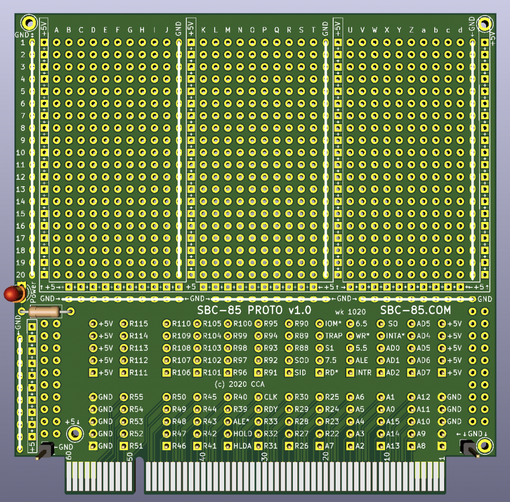
- 100mm x 100mm 2-layer PCB
- All bus signals including reserved (unused) are brought out to pads
- +5V and GND test points including loops for test clips and pins for DuPont connectors
- Three component areas, each with 200 pad-per-holes
- Each component area is surrounded on 3-sides with rows of +5V and GND pads
- +5V pads are square, 0V pads are ovals, and unconnected pads are circles
- Labels, Labels, Labels. Every +5V pad has a + nearby and every GND pad has a — nearby
- Place for a power LED and resistor
So let me know… Anything else you would like to see added or changed before these go to the fab house?